S02_CH15_ AXI_OLED 实验
S02_CH15_ AXI_OLED 实验
在上一个例子中,主要是以软件功能为主,采用了软件模拟SPI时序进行控制OLED。这样做的好处是灵活,但是牺牲了效率。本章采用的方式是让SPI驱动由Verilog实现,字库也是保存到了PL部分的BRAM中。这种方式是减轻了CPU负担,提高了CPU效率。缺点是没有上一章的方法灵活。
15.1 自定义IP的封装
Step1:新建一个名为Miz_sys空的工程。
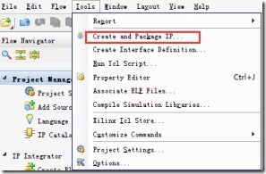
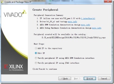
Step2:选择Tools Create and Package IP 创建IP
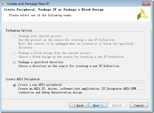
Step3:单击NEXT

Step4:由于我们需要挂在到总线上,因此创建一个带AXI总线的用户IP
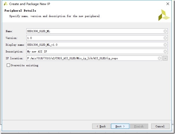
Step5:设置IP的名字为SSD1306_OLED_ML版本号默认,并且记住IP的位置
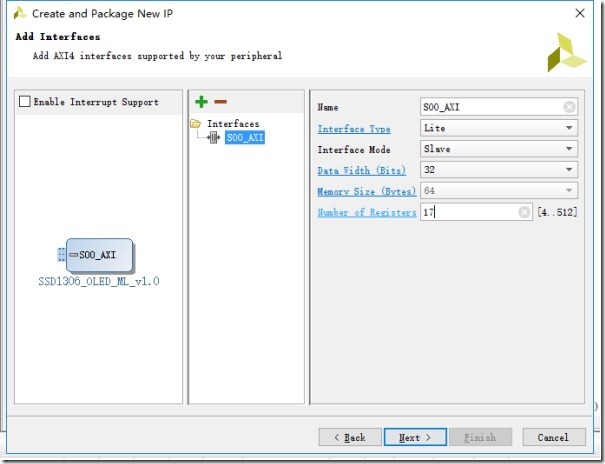
Step6:设置总线形式为Lite总线,Lite总线是简化的AXI总线消耗的资源少,当然性能也是比完全版的AXI总线差一点,但是由于音频的速度并不高,因此采用Lite总线就够了,设置寄存器数量为17,因为后面我们需要用到17个寄存器。
Step7:选择Edit IP单击Finish完成
15.2 SSD1306_OLED_ML用户IP的修改
IP创建完成后,并不能立马使用,还需要做一些修改。
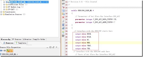
Step1:打开SSD1306_OLED_ML.v文件在以下位置修改:
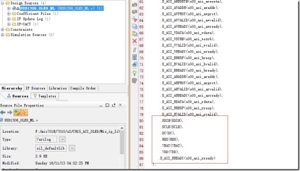
Step2:用以下程序替代SSD1306_OLED_ML_v1_0_S00_AXI.v。
|
`timescale 1 ns / 1 ps ////////////////////////////////////////////////////////////////////////////////// // // // Create Date: 06:13:25 08/18/2014 // Module Name: SSD1306_OLED_v1_0_S00_AXI // Project Name: SSD1306_OLED // Target Devices: Zynq // Tool versions: Vivado 14.2 (64-bits) // Description: The core is a slave AXI peripheral with 17 software-accessed registers. // registers 0-16 are used for data, register 17 is the control register // // Revision: 1.0 - SSD1306_OLED_v1_0_S00_AXI completed // Revision 0.01 - File Created // ////////////////////////////////////////////////////////////////////////////////// module SSD1306_OLED_v1_0_S00_AXI # ( // Width of S_AXI data bus parameter integer C_S_AXI_DATA_WIDTH = 32, // Width of S_AXI address bus parameter integer C_S_AXI_ADDR_WIDTH = 7 ) ( // Interface with the SSD1306 starts here //SPI Data In (MOSI) output SDIN, //SPI Clock output SCLK, //Data_Command Control output DC, //Power Reset output RES, //Battery Voltage Control - connected to field-effect transistors-active low output VBAT, // Logic Voltage Control - connected to field-effect transistors-active low output VDD, // Interface with the SSD1306 ends here // Global Clock Signal input wire S_AXI_ACLK, // Global Reset Signal. This Signal is Active LOW input wire S_AXI_ARESETN, // Write address (issued by master, acceped by Slave) input wire [C_S_AXI_ADDR_WIDTH-1 : 0] S_AXI_AWADDR, // Write channel Protection type. This signal indicates the // privilege and security level of the transaction, and whether // the transaction is a data access or an instruction access. input wire [2 : 0] S_AXI_AWPROT, // Write address valid. This signal indicates that the master signaling // valid write address and control information. input wire S_AXI_AWVALID, // Write address ready. This signal indicates that the slave is ready // to accept an address and associated control signals. output wire S_AXI_AWREADY, // Write data (issued by master, acceped by Slave) input wire [C_S_AXI_DATA_WIDTH-1 : 0] S_AXI_WDATA, // Write strobes. This signal indicates which byte lanes hold // valid data. There is one write strobe bit for each eight // bits of the write data bus. input wire [(C_S_AXI_DATA_WIDTH/8)-1 : 0] S_AXI_WSTRB, // Write valid. This signal indicates that valid write // data and strobes are available. input wire S_AXI_WVALID, // Write ready. This signal indicates that the slave // can accept the write data. output wire S_AXI_WREADY, // Write response. This signal indicates the status // of the write transaction. output wire [1 : 0] S_AXI_BRESP, // Write response valid. This signal indicates that the channel // is signaling a valid write response. output wire S_AXI_BVALID, // Response ready. This signal indicates that the master // can accept a write response. input wire S_AXI_BREADY, // Read address (issued by master, acceped by Slave) input wire [C_S_AXI_ADDR_WIDTH-1 : 0] S_AXI_ARADDR, // Protection type. This signal indicates the privilege // and security level of the transaction, and whether the // transaction is a data access or an instruction access. input wire [2 : 0] S_AXI_ARPROT, // Read address valid. This signal indicates that the channel // is signaling valid read address and control information. input wire S_AXI_ARVALID, // Read address ready. This signal indicates that the slave is // ready to accept an address and associated control signals. output wire S_AXI_ARREADY, // Read data (issued by slave) output wire [C_S_AXI_DATA_WIDTH-1 : 0] S_AXI_RDATA, // Read response. This signal indicates the status of the // read transfer. output wire [1 : 0] S_AXI_RRESP, // Read valid. This signal indicates that the channel is // signaling the required read data. output wire S_AXI_RVALID, // Read ready. This signal indicates that the master can // accept the read data and response information. input wire S_AXI_RREADY ); // AXI4LITE signals reg [C_S_AXI_ADDR_WIDTH-1 : 0] axi_awaddr; reg axi_awready; reg axi_wready; reg [1 : 0] axi_bresp; reg axi_bvalid; reg [C_S_AXI_ADDR_WIDTH-1 : 0] axi_araddr; reg axi_arready; reg [C_S_AXI_DATA_WIDTH-1 : 0] axi_rdata; reg [1 : 0] axi_rresp; reg axi_rvalid; // Example-specific design signals // local parameter for addressing 32 bit / 64 bit C_S_AXI_DATA_WIDTH // ADDR_LSB is used for addressing 32/64 bit registers/memories // ADDR_LSB = 2 for 32 bits (n downto 2) // ADDR_LSB = 3 for 64 bits (n downto 3) localparam integer ADDR_LSB = (C_S_AXI_DATA_WIDTH/32) + 1; localparam integer OPT_MEM_ADDR_BITS = 4; //---------------------------------------------- //-- Signals for user logic register space example //------------------------------------------------ //-- Number of Slave Registers 17 reg [C_S_AXI_DATA_WIDTH-1:0] slv_reg0; reg [C_S_AXI_DATA_WIDTH-1:0] slv_reg1; reg [C_S_AXI_DATA_WIDTH-1:0] slv_reg2; reg [C_S_AXI_DATA_WIDTH-1:0] slv_reg3; reg [C_S_AXI_DATA_WIDTH-1:0] slv_reg4; reg [C_S_AXI_DATA_WIDTH-1:0] slv_reg5; reg [C_S_AXI_DATA_WIDTH-1:0] slv_reg6; reg [C_S_AXI_DATA_WIDTH-1:0] slv_reg7; reg [C_S_AXI_DATA_WIDTH-1:0] slv_reg8; reg [C_S_AXI_DATA_WIDTH-1:0] slv_reg9; reg [C_S_AXI_DATA_WIDTH-1:0] slv_reg10; reg [C_S_AXI_DATA_WIDTH-1:0] slv_reg11; reg [C_S_AXI_DATA_WIDTH-1:0] slv_reg12; reg [C_S_AXI_DATA_WIDTH-1:0] slv_reg13; reg [C_S_AXI_DATA_WIDTH-1:0] slv_reg14; reg [C_S_AXI_DATA_WIDTH-1:0] slv_reg15; reg [C_S_AXI_DATA_WIDTH-1:0] slv_reg16; wire slv_reg_rden; wire slv_reg_wren; reg [C_S_AXI_DATA_WIDTH-1:0] reg_data_out; integer byte_index; // I/O Connections assignments assign S_AXI_AWREADY = axi_awready; assign S_AXI_WREADY = axi_wready; assign S_AXI_BRESP = axi_bresp; assign S_AXI_BVALID = axi_bvalid; assign S_AXI_ARREADY = axi_arready; assign S_AXI_RDATA = axi_rdata; assign S_AXI_RRESP = axi_rresp; assign S_AXI_RVALID = axi_rvalid; // Implement axi_awready generation // axi_awready is asserted for one S_AXI_ACLK clock cycle when both // S_AXI_AWVALID and S_AXI_WVALID are asserted. axi_awready is // de-asserted when reset is low. // =========================================================================== // Parameters, Regsiters, and Wires // =========================================================================== //Current overall state of the state machine reg [143:0] current_state; //State to go to after the SPI transmission is finished reg [111:0] after_state; //State to go to after the set page sequence reg [142:0] after_page_state; //State to go to after sending the character sequence reg [95:0] after_char_state; //State to go to after the UpdateScreen is finished reg [39:0] after_update_state; //Variable that contains what the screen will be after the next UpdateScreen state reg [7:0] current_screen[0:3][0:15]; //Variable assigned to the SSD1306 interface reg temp_dc = 1'b0; reg temp_res = 1'b1; reg temp_vbat = 1'b1; reg temp_vdd = 1'b1; assign DC = temp_dc; assign RES = temp_res; assign VBAT = temp_vbat; assign VDD = temp_vdd; //-------------- Variables used in the Delay Controller Block -------------- wire [11:0] temp_delay_ms; //amount of ms to delay reg temp_delay_en = 1'b0; //Enable signal for the delay block wire temp_delay_fin; //Finish signal for the delay block assign temp_delay_ms = (after_state == "DispContrast1") ? 12'h074 : 12'h014; //-------------- Variables used in the SPI controller block ---------------- reg temp_spi_en = 1'b0; //Enable signal for the SPI block reg [7:0] temp_spi_data = 8'h00; //Data to be sent out on SPI wire temp_spi_fin; //Finish signal for the SPI block //-------------- Variables used in the characters libtray ---------------- reg [7:0] temp_char; //Contains ASCII value for character reg [10:0] temp_addr; //Contains address to BYTE needed in memory wire [7:0] temp_dout; //Contains byte outputted from memory reg [1:0] temp_page; //Current page reg [3:0] temp_index; //Current character on page //-------------- Variables used in the reset and synchronization circuitry ---------------- reg init_first_r = 1'b1; // Initilaize only one time reg clear_screen_i = 1'b1; // Clear the screen on start up reg ready = 1'b0; // Ready flag reg RST_internal =1'b1; reg[11:0] count =12'h000; wire RST_IN; wire RST=1'b0; // dummy wire - can be connected as a port to provide external reset to the circuit integer i = 0; integer j = 0; assign RST_IN = (RST || RST_internal); //-------------- Core commands assignments start ---------------- wire Display_c; wire Clear_c; assign Display_c = slv_reg16[0]; assign Clear_c =slv_reg16[1]; //-------------- Core commands assignments end ---------------- always @( posedge S_AXI_ACLK ) begin if ( S_AXI_ARESETN == 1'b0 ) begin axi_awready <= 1'b0; end else begin if (~axi_awready && S_AXI_AWVALID && S_AXI_WVALID) begin // slave is ready to accept write address when // there is a valid write address and write data // on the write address and data bus. This design // expects no outstanding transactions. axi_awready <= 1'b1; end else begin axi_awready <= 1'b0; end end end // Implement axi_awaddr latching // This process is used to latch the address when both // S_AXI_AWVALID and S_AXI_WVALID are valid. always @( posedge S_AXI_ACLK ) begin if ( S_AXI_ARESETN == 1'b0 ) begin axi_awaddr <= 0; end else begin if (~axi_awready && S_AXI_AWVALID && S_AXI_WVALID) begin // Write Address latching axi_awaddr <= S_AXI_AWADDR; end end end // Implement axi_wready generation // axi_wready is asserted for one S_AXI_ACLK clock cycle when both // S_AXI_AWVALID and S_AXI_WVALID are asserted. axi_wready is // de-asserted when reset is low. always @( posedge S_AXI_ACLK ) begin if ( S_AXI_ARESETN == 1'b0 ) begin axi_wready <= 1'b0; end else begin if (~axi_wready && S_AXI_WVALID && S_AXI_AWVALID) begin // slave is ready to accept write data when // there is a valid write address and write data // on the write address and data bus. This design // expects no outstanding transactions. axi_wready <= 1'b1; end else begin axi_wready <= 1'b0; end end end // Implement memory mapped register select and write logic generation // The write data is accepted and written to memory mapped registers when // axi_awready, S_AXI_WVALID, axi_wready and S_AXI_WVALID are asserted. Write strobes are used to // select byte enables of slave registers while writing. // These registers are cleared when reset (active low) is applied. // Slave register write enable is asserted when valid address and data are available // and the slave is ready to accept the write address and write data. assign slv_reg_wren = axi_wready && S_AXI_WVALID && axi_awready && S_AXI_AWVALID; always @( posedge S_AXI_ACLK ) begin if ( S_AXI_ARESETN == 1'b0 ) begin slv_reg0 <= 0; slv_reg1 <= 0; slv_reg2 <= 0; slv_reg3 <= 0; slv_reg4 <= 0; slv_reg5 <= 0; slv_reg6 <= 0; slv_reg7 <= 0; slv_reg8 <= 0; slv_reg9 <= 0; slv_reg10 <= 0; slv_reg11 <= 0; slv_reg12 <= 0; slv_reg13 <= 0; slv_reg14 <= 0; slv_reg15 <= 0; slv_reg16 <= 0; end else begin if (slv_reg_wren) begin case ( axi_awaddr[ADDR_LSB+OPT_MEM_ADDR_BITS:ADDR_LSB] ) 5'h00: for ( byte_index = 0; byte_index <= (C_S_AXI_DATA_WIDTH/8)-1; byte_index = byte_index+1 ) if ( S_AXI_WSTRB[byte_index] == 1 ) begin // Respective byte enables are asserted as per write strobes // Slave register 0 slv_reg0[(byte_index*8) +: 8] <= S_AXI_WDATA[(byte_index*8) +: 8]; end 5'h01: for ( byte_index = 0; byte_index <= (C_S_AXI_DATA_WIDTH/8)-1; byte_index = byte_index+1 ) if ( S_AXI_WSTRB[byte_index] == 1 ) begin // Respective byte enables are asserted as per write strobes // Slave register 1 slv_reg1[(byte_index*8) +: 8] <= S_AXI_WDATA[(byte_index*8) +: 8]; end 5'h02: for ( byte_index = 0; byte_index <= (C_S_AXI_DATA_WIDTH/8)-1; byte_index = byte_index+1 ) if ( S_AXI_WSTRB[byte_index] == 1 ) begin // Respective byte enables are asserted as per write strobes // Slave register 2 slv_reg2[(byte_index*8) +: 8] <= S_AXI_WDATA[(byte_index*8) +: 8]; end 5'h03: for ( byte_index = 0; byte_index <= (C_S_AXI_DATA_WIDTH/8)-1; byte_index = byte_index+1 ) if ( S_AXI_WSTRB[byte_index] == 1 ) begin // Respective byte enables are asserted as per write strobes // Slave register 3 slv_reg3[(byte_index*8) +: 8] <= S_AXI_WDATA[(byte_index*8) +: 8]; end 5'h04: for ( byte_index = 0; byte_index <= (C_S_AXI_DATA_WIDTH/8)-1; byte_index = byte_index+1 ) if ( S_AXI_WSTRB[byte_index] == 1 ) begin // Respective byte enables are asserted as per write strobes // Slave register 4 slv_reg4[(byte_index*8) +: 8] <= S_AXI_WDATA[(byte_index*8) +: 8]; end 5'h05: for ( byte_index = 0; byte_index <= (C_S_AXI_DATA_WIDTH/8)-1; byte_index = byte_index+1 ) if ( S_AXI_WSTRB[byte_index] == 1 ) begin // Respective byte enables are asserted as per write strobes // Slave register 5 slv_reg5[(byte_index*8) +: 8] <= S_AXI_WDATA[(byte_index*8) +: 8]; end 5'h06: for ( byte_index = 0; byte_index <= (C_S_AXI_DATA_WIDTH/8)-1; byte_index = byte_index+1 ) if ( S_AXI_WSTRB[byte_index] == 1 ) begin // Respective byte enables are asserted as per write strobes // Slave register 6 slv_reg6[(byte_index*8) +: 8] <= S_AXI_WDATA[(byte_index*8) +: 8]; end 5'h07: for ( byte_index = 0; byte_index <= (C_S_AXI_DATA_WIDTH/8)-1; byte_index = byte_index+1 ) if ( S_AXI_WSTRB[byte_index] == 1 ) begin // Respective byte enables are asserted as per write strobes // Slave register 7 slv_reg7[(byte_index*8) +: 8] <= S_AXI_WDATA[(byte_index*8) +: 8]; end 5'h08: for ( byte_index = 0; byte_index <= (C_S_AXI_DATA_WIDTH/8)-1; byte_index = byte_index+1 ) if ( S_AXI_WSTRB[byte_index] == 1 ) begin // Respective byte enables are asserted as per write strobes // Slave register 8 slv_reg8[(byte_index*8) +: 8] <= S_AXI_WDATA[(byte_index*8) +: 8]; end 5'h09: for ( byte_index = 0; byte_index <= (C_S_AXI_DATA_WIDTH/8)-1; byte_index = byte_index+1 ) if ( S_AXI_WSTRB[byte_index] == 1 ) begin // Respective byte enables are asserted as per write strobes // Slave register 9 slv_reg9[(byte_index*8) +: 8] <= S_AXI_WDATA[(byte_index*8) +: 8]; end 5'h0A: for ( byte_index = 0; byte_index <= (C_S_AXI_DATA_WIDTH/8)-1; byte_index = byte_index+1 ) if ( S_AXI_WSTRB[byte_index] == 1 ) begin // Respective byte enables are asserted as per write strobes // Slave register 10 slv_reg10[(byte_index*8) +: 8] <= S_AXI_WDATA[(byte_index*8) +: 8]; end 5'h0B: for ( byte_index = 0; byte_index <= (C_S_AXI_DATA_WIDTH/8)-1; byte_index = byte_index+1 ) if ( S_AXI_WSTRB[byte_index] == 1 ) begin // Respective byte enables are asserted as per write strobes // Slave register 11 slv_reg11[(byte_index*8) +: 8] <= S_AXI_WDATA[(byte_index*8) +: 8]; end 5'h0C: for ( byte_index = 0; byte_index <= (C_S_AXI_DATA_WIDTH/8)-1; byte_index = byte_index+1 ) if ( S_AXI_WSTRB[byte_index] == 1 ) begin // Respective byte enables are asserted as per write strobes // Slave register 12 slv_reg12[(byte_index*8) +: 8] <= S_AXI_WDATA[(byte_index*8) +: 8]; end 5'h0D: for ( byte_index = 0; byte_index <= (C_S_AXI_DATA_WIDTH/8)-1; byte_index = byte_index+1 ) if ( S_AXI_WSTRB[byte_index] == 1 ) begin // Respective byte enables are asserted as per write strobes // Slave register 13 slv_reg13[(byte_index*8) +: 8] <= S_AXI_WDATA[(byte_index*8) +: 8]; end 5'h0E: for ( byte_index = 0; byte_index <= (C_S_AXI_DATA_WIDTH/8)-1; byte_index = byte_index+1 ) if ( S_AXI_WSTRB[byte_index] == 1 ) begin // Respective byte enables are asserted as per write strobes // Slave register 14 slv_reg14[(byte_index*8) +: 8] <= S_AXI_WDATA[(byte_index*8) +: 8]; end 5'h0F: for ( byte_index = 0; byte_index <= (C_S_AXI_DATA_WIDTH/8)-1; byte_index = byte_index+1 ) if ( S_AXI_WSTRB[byte_index] == 1 ) begin // Respective byte enables are asserted as per write strobes // Slave register 15 slv_reg15[(byte_index*8) +: 8] <= S_AXI_WDATA[(byte_index*8) +: 8]; end 5'h10: for ( byte_index = 0; byte_index <= (C_S_AXI_DATA_WIDTH/8)-1; byte_index = byte_index+1 ) if ( S_AXI_WSTRB[byte_index] == 1 ) begin // Respective byte enables are asserted as per write strobes // Slave register 16 slv_reg16[(byte_index*8) +: 8] <= S_AXI_WDATA[(byte_index*8) +: 8]; end default : begin slv_reg0 <= slv_reg0; slv_reg1 <= slv_reg1; slv_reg2 <= slv_reg2; slv_reg3 <= slv_reg3; slv_reg4 <= slv_reg4; slv_reg5 <= slv_reg5; slv_reg6 <= slv_reg6; slv_reg7 <= slv_reg7; slv_reg8 <= slv_reg8; slv_reg9 <= slv_reg9; slv_reg10 <= slv_reg10; slv_reg11 <= slv_reg11; slv_reg12 <= slv_reg12; slv_reg13 <= slv_reg13; slv_reg14 <= slv_reg14; slv_reg15 <= slv_reg15; slv_reg16 <= slv_reg16; end endcase end end end // Implement write response logic generation // The write response and response valid signals are asserted by the slave // when axi_wready, S_AXI_WVALID, axi_wready and S_AXI_WVALID are asserted. // This marks the acceptance of address and indicates the status of // write transaction. always @( posedge S_AXI_ACLK ) begin if ( S_AXI_ARESETN == 1'b0 ) begin axi_bvalid <= 0; axi_bresp <= 2'b0; end else begin if (axi_awready && S_AXI_AWVALID && ~axi_bvalid && axi_wready && S_AXI_WVALID) begin // indicates a valid write response is available axi_bvalid <= 1'b1; axi_bresp <= 2'b0; // 'OKAY' response end // work error responses in future else begin if (S_AXI_BREADY && axi_bvalid) //check if bready is asserted while bvalid is high) //(there is a possibility that bready is always asserted high) begin axi_bvalid <= 1'b0; end end end end // Implement axi_arready generation // axi_arready is asserted for one S_AXI_ACLK clock cycle when // S_AXI_ARVALID is asserted. axi_awready is // de-asserted when reset (active low) is asserted. // The read address is also latched when S_AXI_ARVALID is // asserted. axi_araddr is reset to zero on reset assertion. always @( posedge S_AXI_ACLK ) begin if ( S_AXI_ARESETN == 1'b0 ) begin axi_arready <= 1'b0; axi_araddr <= 32'b0; end else begin if (~axi_arready && S_AXI_ARVALID) begin // indicates that the slave has acceped the valid read address axi_arready <= 1'b1; // Read address latching axi_araddr <= S_AXI_ARADDR; end else begin axi_arready <= 1'b0; end end end // Implement axi_arvalid generation // axi_rvalid is asserted for one S_AXI_ACLK clock cycle when both // S_AXI_ARVALID and axi_arready are asserted. The slave registers // data are available on the axi_rdata bus at this instance. The // assertion of axi_rvalid marks the validity of read data on the // bus and axi_rresp indicates the status of read transaction.axi_rvalid // is deasserted on reset (active low). axi_rresp and axi_rdata are // cleared to zero on reset (active low). always @( posedge S_AXI_ACLK ) begin if ( S_AXI_ARESETN == 1'b0 ) begin axi_rvalid <= 0; axi_rresp <= 0; end else begin if (axi_arready && S_AXI_ARVALID && ~axi_rvalid) begin // Valid read data is available at the read data bus axi_rvalid <= 1'b1; axi_rresp <= 2'b0; // 'OKAY' response end else if (axi_rvalid && S_AXI_RREADY) begin // Read data is accepted by the master axi_rvalid <= 1'b0; end end end // Implement memory mapped register select and read logic generation // Slave register read enable is asserted when valid address is available // and the slave is ready to accept the read address. assign slv_reg_rden = axi_arready & S_AXI_ARVALID & ~axi_rvalid; always @(*) begin if ( S_AXI_ARESETN == 1'b0 ) begin reg_data_out <= 0; end else begin // Address decoding for reading registers case ( axi_araddr[ADDR_LSB+OPT_MEM_ADDR_BITS:ADDR_LSB] ) 5'h00 : reg_data_out <= slv_reg0; 5'h01 : reg_data_out <= slv_reg1; 5'h02 : reg_data_out <= slv_reg2; 5'h03 : reg_data_out <= slv_reg3; 5'h04 : reg_data_out <= slv_reg4; 5'h05 : reg_data_out <= slv_reg5; 5'h06 : reg_data_out <= slv_reg6; 5'h07 : reg_data_out <= slv_reg7; 5'h08 : reg_data_out <= slv_reg8; 5'h09 : reg_data_out <= slv_reg9; 5'h0A : reg_data_out <= slv_reg10; 5'h0B : reg_data_out <= slv_reg11; 5'h0C : reg_data_out <= slv_reg12; 5'h0D : reg_data_out <= slv_reg13; 5'h0E : reg_data_out <= slv_reg14; 5'h0F : reg_data_out <= slv_reg15; 5'h10 : reg_data_out <= slv_reg16; default : reg_data_out <= 0; endcase end end // Output register or memory read data always @( posedge S_AXI_ACLK ) begin if ( S_AXI_ARESETN == 1'b0 ) begin axi_rdata <= 0; end else begin // When there is a valid read address (S_AXI_ARVALID) with // acceptance of read address by the slave (axi_arready), // output the read dada if (slv_reg_rden) begin axi_rdata <= reg_data_out; // register read data end end end // =========================================================================== // Implementation // =========================================================================== SpiCtrl SPI_COMP( .CLK(S_AXI_ACLK), .RST(RST_IN), .SPI_EN(temp_spi_en), .SPI_DATA(temp_spi_data), .SDO(SDIN), .SCLK(SCLK), .SPI_FIN(temp_spi_fin) ); Delay DELAY_COMP( .CLK(S_AXI_ACLK), .RST(RST_IN), .DELAY_MS(temp_delay_ms), .DELAY_EN(temp_delay_en), .DELAY_FIN(temp_delay_fin) ); charLib CHAR_LIB_COMP( .clka(S_AXI_ACLK), .addra(temp_addr), .douta(temp_dout) ); // State Machine always @(posedge S_AXI_ACLK) begin if(RST_IN == 1'b1) begin current_state <= "Idle"; temp_res <= 1'b0; end else begin temp_res <= 1'b1; case(current_state) // Idle State "Idle" : begin if(init_first_r == 1'b1) begin temp_dc <= 1'b0; // DC= 0 "Commands" , DC=1 "Data" current_state <= "VddOn"; init_first_r <= 1'b0; // Don't go over the initialization more than once end else begin current_state <="WaitRequest"; end end // Initialization Sequence // This should be done only one time when Zedboard starts "VddOn" : begin // turn the power on the logic of the display temp_vdd <= 1'b0; // remember the power FET transistor for VDD is active low current_state <= "Wait1"; end // 3 "Wait1" : begin after_state <= "DispOff"; current_state <= "Transition3"; end // 4 "DispOff" : begin temp_spi_data <= 8'hAE; // 0xAE= Set Display OFF after_state <= "SetClockDiv1"; current_state <= "Transition1"; end // 5 "SetClockDiv1" : begin temp_spi_data <= 8'hD5; //0xD5 after_state <= "SetClockDiv2"; current_state <= "Transition1"; end // 6 "SetClockDiv2" : begin temp_spi_data <= 8'h80; // 0x80 after_state <= "MultiPlex1"; current_state <= "Transition1"; end // 7 "MultiPlex1" : begin temp_spi_data <= 8'hA8; //0xA8 after_state <= "MultiPlex2"; current_state <= "Transition1"; end // 8 "MultiPlex2" : begin temp_spi_data <= 8'h1F; // 0x1F after_state <= "ChargePump1"; current_state <= "Transition1"; end // 9 "ChargePump1" : begin // Access Charge Pump Setting temp_spi_data <= 8'h8D; //0x8D after_state <= "ChargePump2"; current_state <= "Transition1"; end // 10 "ChargePump2" : begin // Enable Charge Pump temp_spi_data <= 8'h14; // 0x14 after_state <= "PreCharge1"; current_state <= "Transition1"; end // 11 "PreCharge1" : begin // Access Pre-charge Period Setting temp_spi_data <= 8'hD9; // 0xD9 after_state <= "PreCharge2"; current_state <= "Transition1"; end // 12 "PreCharge2" : begin //Set the Pre-charge Period temp_spi_data <= 8'hFF; // 0xF1 after_state <= "VCOMH1"; current_state <= "Transition1"; end // 13 "VCOMH1" : begin //Set the Pre-charge Period temp_spi_data <= 8'hDB; // 0xF1 after_state <= "VCOMH2"; current_state <= "Transition1"; end // 14 "VCOMH2" : begin //Set the Pre-charge Period temp_spi_data <= 8'h40; // 0xF1 after_state <= "DispContrast1"; current_state <= "Transition1"; end // 15 "DispContrast1" : begin //Set Contrast Control for BANK0 temp_spi_data <= 8'h81; // 0x81 after_state <= "DispContrast2"; current_state <= "Transition1"; end // 16 "DispContrast2" : begin temp_spi_data <= 8'hF1; // 0x0F after_state <= "InvertDisp1"; current_state <= "Transition1"; end // 17 "InvertDisp1" : begin temp_spi_data <= 8'hA0; // 0xA1 after_state <= "InvertDisp2"; current_state <= "Transition1"; end // 18 "InvertDisp2" : begin temp_spi_data <= 8'hC0; // 0xC0 after_state <= "ComConfig1"; current_state <= "Transition1"; end // 19 "ComConfig1" : begin temp_spi_data <= 8'hDA; // 0xDA after_state <= "ComConfig2"; current_state <= "Transition1"; end // 20 "ComConfig2" : begin temp_spi_data <= 8'h02; // 0x02 after_state <= "VbatOn"; current_state <= "Transition1"; end // 21 "VbatOn" : begin temp_vbat <= 1'b0; current_state <= "Wait3"; end // 22 "Wait3" : begin after_state <= "ResetOn"; current_state <= "Transition3"; end // 23 "ResetOn" : begin temp_res <= 1'b0; current_state <= "Wait2"; end // 24 "Wait2" : begin after_state <= "ResetOff"; current_state <= "Transition3"; end // 25 "ResetOff" : begin temp_res <= 1'b1; current_state <= "WaitRequest"; end // ************ END Initialization sequence but without turnning the dispay on ************ // Main state "WaitRequest" : begin if(Display_c == 1'b1) begin current_state <= "ClearDC"; after_page_state <= "ReadRegisters"; temp_page <= 2'b00; end else if ((Clear_c==1'b1) || (clear_screen_i == 1'b1)) begin current_state <= "ClearDC"; after_page_state <= "ClearScreen"; temp_page <= 2'b00; end else begin current_state<="WaitRequest"; // keep looping in the WaitRequest state untill you receive a command if ((clear_screen_i == 1'b0) && (ready ==1'b0)) begin // this part is only executed once, on start-up temp_spi_data <= 8'hAF; // 0xAF // Dispaly ON after_state <= "WaitRequest"; current_state <= "Transition1"; temp_dc<=1'b0; ready <= 1'b1; end end end //Update Page states //1. Sets DC to command mode //2. Sends the SetPage Command //3. Sends the Page to be set to //4. Sets the start pixel to the left column //5. Sets DC to data mode "ClearDC" : begin temp_dc <= 1'b0; current_state <= "SetPage"; end "SetPage" : begin temp_spi_data <= 8'b00100010; after_state <= "PageNum"; current_state <= "Transition1"; end "PageNum" : begin temp_spi_data <= {6'b000000,temp_page}; after_state <= "LeftColumn1"; current_state <= "Transition1"; end "LeftColumn1" : begin temp_spi_data <= 8'b00000000; after_state <= "LeftColumn2"; current_state <= "Transition1"; end "LeftColumn2" : begin temp_spi_data <= 8'b00010000; after_state <= "SetDC"; current_state <= "Transition1"; end "SetDC" : begin temp_dc <= 1'b1; current_state <= after_page_state; end "ClearScreen" : begin for(i = 0; i <= 3 ; i=i+1) begin for(j = 0; j <= 15 ; j=j+1) begin current_screen[i][j] <= 8'h20; end end after_update_state <= "WaitRequest"; current_state <= "UpdateScreen"; end "ReadRegisters" : begin // Page0 current_screen[0][0]<=slv_reg0[7:0]; current_screen[0][1]<=slv_reg0[15:8]; current_screen[0][2]<=slv_reg0[23:16]; current_screen[0][3]<=slv_reg0[31:24]; current_screen[0][4]<=slv_reg1[7:0]; current_screen[0][5]<=slv_reg1[15:8]; current_screen[0][6]<=slv_reg1[23:16]; current_screen[0][7]<=slv_reg1[31:24]; current_screen[0][8]<=slv_reg2[7:0]; current_screen[0][9]<=slv_reg2[15:8]; current_screen[0][10]<=slv_reg2[23:16]; current_screen[0][11]<=slv_reg2[31:24]; current_screen[0][12]<=slv_reg3[7:0]; current_screen[0][13]<=slv_reg3[15:8]; current_screen[0][14]<=slv_reg3[23:16]; current_screen[0][15]<=slv_reg3[31:24]; //Page1 current_screen[1][0]<=slv_reg4[7:0]; current_screen[1][1]<=slv_reg4[15:8]; current_screen[1][2]<=slv_reg4[23:16]; current_screen[1][3]<=slv_reg4[31:24]; current_screen[1][4]<=slv_reg5[7:0]; current_screen[1][5]<=slv_reg5[15:8]; current_screen[1][6]<=slv_reg5[23:16]; current_screen[1][7]<=slv_reg5[31:24]; current_screen[1][8]<=slv_reg6[7:0]; current_screen[1][9]<=slv_reg6[15:8]; current_screen[1][10]<=slv_reg6[23:16]; current_screen[1][11]<=slv_reg6[31:24]; current_screen[1][12]<=slv_reg7[7:0]; current_screen[1][13]<=slv_reg7[15:8]; current_screen[1][14]<=slv_reg7[23:16]; current_screen[1][15]<=slv_reg7[31:24]; //Page2 current_screen[2][0]<=slv_reg8[7:0]; current_screen[2][1]<=slv_reg8[15:8]; current_screen[2][2]<=slv_reg8[23:16]; current_screen[2][3]<=slv_reg8[31:24]; current_screen[2][4]<=slv_reg9[7:0]; current_screen[2][5]<=slv_reg9[15:8]; current_screen[2][6]<=slv_reg9[23:16]; current_screen[2][7]<=slv_reg9[31:24]; current_screen[2][8]<=slv_reg10[7:0]; current_screen[2][9]<=slv_reg10[15:8]; current_screen[2][10]<=slv_reg10[23:16]; current_screen[2][11]<=slv_reg10[31:24]; current_screen[2][12]<=slv_reg11[7:0]; current_screen[2][13]<=slv_reg11[15:8]; current_screen[2][14]<=slv_reg11[23:16]; current_screen[2][15]<=slv_reg11[31:24]; //Page3 current_screen[3][0]<=slv_reg12[7:0]; current_screen[3][1]<=slv_reg12[15:8]; current_screen[3][2]<=slv_reg12[23:16]; current_screen[3][3]<=slv_reg12[31:24]; current_screen[3][4]<=slv_reg13[7:0]; current_screen[3][5]<=slv_reg13[15:8]; current_screen[3][6]<=slv_reg13[23:16]; current_screen[3][7]<=slv_reg13[31:24]; current_screen[3][8]<=slv_reg14[7:0]; current_screen[3][9]<=slv_reg14[15:8]; current_screen[3][10]<=slv_reg14[23:16]; current_screen[3][11]<=slv_reg14[31:24]; current_screen[3][12]<=slv_reg15[7:0]; current_screen[3][13]<=slv_reg15[15:8]; current_screen[3][14]<=slv_reg15[23:16]; current_screen[3][15]<=slv_reg15[31:24]; after_update_state <= "WaitRequest"; current_state <= "UpdateScreen"; end //UpdateScreen State //1. Gets ASCII value from current_screen at the current page and the current spot of the page //2. If on the last character of the page transition update the page number, if on the last page(3) // then the updateScreen go to "after_update_state" after "UpdateScreen" : begin temp_char <= current_screen[temp_page][temp_index]; if(temp_index == 'd15) begin temp_index <= 'd0; temp_page <= temp_page + 1'b1; after_char_state <= "ClearDC"; if(temp_page == 2'b11) begin after_page_state <= after_update_state; clear_screen_i<=1'b0; end else begin after_page_state <= "UpdateScreen"; end end else begin temp_index <= temp_index + 1'b1; after_char_state <= "UpdateScreen"; end current_state <= "SendChar1"; end //Send Character States //1. Sets the Address to ASCII value of char with the counter appended to the end //2. Waits a clock for the data to get ready by going to ReadMem and ReadMem2 states //3. Send the byte of data given by the block Ram //4. Repeat 7 more times for the rest of the character bytes "SendChar1" : begin temp_addr <= {temp_char, 3'b000}; after_state <= "SendChar2"; current_state <= "ReadMem"; end "SendChar2" : begin temp_addr <= {temp_char, 3'b001}; after_state <= "SendChar3"; current_state <= "ReadMem"; end "SendChar3" : begin temp_addr <= {temp_char, 3'b010}; after_state <= "SendChar4"; current_state <= "ReadMem"; end "SendChar4" : begin temp_addr <= {temp_char, 3'b011}; after_state <= "SendChar5"; current_state <= "ReadMem"; end "SendChar5" : begin temp_addr <= {temp_char, 3'b100}; after_state <= "SendChar6"; current_state <= "ReadMem"; end "SendChar6" : begin temp_addr <= {temp_char, 3'b101}; after_state <= "SendChar7"; current_state <= "ReadMem"; end "SendChar7" : begin temp_addr <= {temp_char, 3'b110}; after_state <= "SendChar8"; current_state <= "ReadMem"; end "SendChar8" : begin temp_addr <= {temp_char, 3'b111}; after_state <= after_char_state; current_state <= "ReadMem"; end "ReadMem" : begin current_state <= "ReadMem2"; end "ReadMem2" : begin temp_spi_data <= temp_dout; current_state <= "Transition1"; end // SPI transitions // 1. Set SPI_EN to 1 // 2. Waits for SpiCtrl to finish // 3. Goes to clear state (Transition5) "Transition1" : begin temp_spi_en <= 1'b1; current_state <= "Transition2"; end "Transition2" : begin if(temp_spi_fin == 1'b1) begin current_state <= "Transition5"; end end // Delay Transitions // 1. Set DELAY_EN to 1 // 2. Waits for Delay to finish // 3. Goes to Clear state (Transition5) "Transition3" : begin temp_delay_en <= 1'b1; current_state <= "Transition4"; end "Transition4" : begin if(temp_delay_fin == 1'b1) begin current_state <= "Transition5"; end end // Clear transition // 1. Sets both DELAY_EN and SPI_EN to 0 // 2. Go to after state "Transition5" : begin temp_spi_en <= 1'b0; temp_delay_en <= 1'b0; current_state <= after_state; end default : current_state <= "Idle"; endcase end end // Internal reset generator always @(posedge S_AXI_ACLK) begin if (RST_IN == 1'b1) count<=count+1'b1; if (count == 12'hFFF) begin RST_internal <=1'b0; end end endmodule |
Step3:添加一个 SPI控制器源码 SpiCtrl.v文件,代码如下所示:
|
`timescale 1ns / 1ps ////////////////////////////////////////////////////////////////////////////////// // // // // // // Create Date: 12:12:51 08/04/2014 // Module Name: SpiCtrl // Project Name: ZedboardOLED // Target Devices: Zynq // Tool versions: Vivado 14.2 (64-bits) // Description: Spi block that sends SPI data formatted SCLK active low with // SDO changing on the falling edge // // Revision: 1.0 - SPI completed // Revision 0.01 - File Created // ////////////////////////////////////////////////////////////////////////////////// module SpiCtrl( CLK, RST, SPI_EN, SPI_DATA, SDO, SCLK, SPI_FIN ); // =========================================================================== // Port Declarations // =========================================================================== input CLK; input RST; input SPI_EN; input [7:0] SPI_DATA; output SDO; output SCLK; output SPI_FIN; // =========================================================================== // Parameters, Regsiters, and Wires // =========================================================================== wire SDO, SCLK, SPI_FIN; reg [39:0] current_state = "Idle"; // Signal for state machine reg [7:0] shift_register = 8'h00; // Shift register to shift out SPI_DATA saved when SPI_EN was set reg [3:0] shift_counter = 4'h0; // Keeps track how many bits were sent wire clk_divided; // Used as SCLK reg [4:0] counter = 5'b00000; // Count clocks to be used to divide CLK reg temp_sdo = 1'b1; // Tied to SDO reg falling = 1'b0; // signal indicating that the clk has just fell // =========================================================================== // Implementation // =========================================================================== assign clk_divided = ~counter[4]; assign SCLK = clk_divided; assign SDO = temp_sdo; assign SPI_FIN = (current_state == "Done") ? 1'b1 : 1'b0; // State Machine always @(posedge CLK) begin if(RST == 1'b1) begin // Synchronous RST current_state <= "Idle"; end else begin case(current_state) // Wait for SPI_EN to go high "Idle" : begin if(SPI_EN == 1'b1) begin current_state <= "Send"; end end // Start sending bits, transition out when all bits are sent and SCLK is high "Send" : begin if(shift_counter == 4'h8 && falling == 1'b0) begin current_state <= "Done"; end end // Finish SPI transimission wait for SPI_EN to go low "Done" : begin if(SPI_EN == 1'b0) begin current_state <= "Idle"; end end default : current_state <= "Idle"; endcase end end // End of State Machine // Clock Divider always @(posedge CLK) begin // start clock counter when in send state if(current_state == "Send") begin counter <= counter + 1'b1; end // reset clock counter when not in send state else begin counter <= 5'b00000; end end // End Clock Divider // SPI_SEND_BYTE, sends SPI data formatted SCLK active low with SDO changing on the falling edge always @(posedge CLK) begin if(current_state == "Idle") begin shift_counter <= 4'h0; // keeps placing SPI_DATA into shift_register so that when state goes to send it has the latest SPI_DATA shift_register <= SPI_DATA; temp_sdo <= 1'b1; end else if(current_state == "Send") begin // if on the falling edge of Clk_divided if(clk_divided == 1'b0 && falling == 1'b0) begin // Indicate that it is passed the falling edge falling <= 1'b1; // send out the MSB temp_sdo <= shift_register[7]; // Shift through SPI_DATA shift_register <= {shift_register[6:0],1'b0}; // Keep track of what bit it is on shift_counter <= shift_counter + 1'b1; end // on SCLK high reset the falling flag else if(clk_divided == 1'b1) begin falling <= 1'b0; end end end endmodule |
这是一个很好用的SPI控制器,只要通过设置 SPI_EN,SPI_DATA,信号就能发送数据了,这个代码初学者可以当作一个verilog的例子学习下,仔细分析下SPI的工作时序。
Step4:添加一个毫秒延迟模块 Delay.v文件
|
`timescale 1ns / 1ps ////////////////////////////////////////////////////////////////////////////////// // // // // // // Create Date: 12:12:51 08/04/2014 // Module Name: Delay // Project Name: ZedboardOLED // Target Devices: Zynq // Tool versions: Vivado 14.2 (64-bits) // Description: Creates a delay of DELAY_MS ms // // Revision: 1.0 // Revision 0.01 - File Created // ////////////////////////////////////////////////////////////////////////////////// module Delay( CLK, RST, DELAY_MS, DELAY_EN, DELAY_FIN ); // =========================================================================== // Port Declarations // =========================================================================== input CLK; input RST; input [11:0] DELAY_MS; input DELAY_EN; output DELAY_FIN; // =========================================================================== // Parameters, Regsiters, and Wires // =========================================================================== wire DELAY_FIN; reg [31:0] current_state = "Idle"; // Signal for state machine reg [16:0] clk_counter = 17'b00000000000000000; // Counts up on every rising edge of CLK reg [11:0] ms_counter = 12'h000; // Counts up when clk_counter = 100,000 // =========================================================================== // Implementation // =========================================================================== assign DELAY_FIN = (current_state == "Done" && DELAY_EN == 1'b1) ? 1'b1 : 1'b0; // State Machine always @(posedge CLK) begin // When RST is asserted switch to idle (synchronous) if(RST == 1'b1) begin current_state <= "Idle"; end else begin case(current_state) "Idle" : begin // Start delay on DELAY_EN if(DELAY_EN == 1'b1) begin current_state <= "Hold"; end end "Hold" : begin // Stay until DELAY_MS has occured if(ms_counter == DELAY_MS) begin current_state <= "Done"; end end "Done" : begin // Wait until DELAY_EN is deasserted to go to IDLE if(DELAY_EN == 1'b0) begin current_state <= "Idle"; end end default : current_state <= "Idle"; endcase end end // End State Machine // Creates ms_counter that counts at 1KHz // CLK_DIV always @(posedge CLK) begin if(current_state == "Hold") begin if(clk_counter == 17'b11000011010100000) begin // 100,000 clk_counter <= 17'b00000000000000000; ms_counter <= ms_counter + 1'b1; // increments at 1KHz end else begin clk_counter <= clk_counter + 1'b1; end end else begin // If not in the hold state reset counters clk_counter <= 17'b00000000000000000; ms_counter <= 12'h000; end end endmodule |
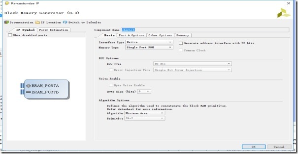
Step5:添加一个Block ROM IP,按下图进行设置。ROM的coe文件可在我们提供的源代码程序包中获得。
Step6:修改完成后重新封装一次自定义IP
Step7:单击NEXT

Step8:和第一次不同,这次选择第一个单选框然后单击NEXT
Step9:选择第一个单选框,然后单击NEXT
Step10:点击Overwrite

Step11:点击Finish 到此自定义IP结束

15.3 OLED硬件控制器关键状态机
|
always @(posedge S_AXI_ACLK) begin if(RST_IN == 1'b1) begin current_state <= "Idle"; temp_res <= 1'b0; end else begin temp_res <= 1'b1; case(current_state) // Idle State "Idle" : begin if(init_first_r == 1'b1) begin temp_dc <= 1'b0; // DC= 0 "Commands" , DC=1 "Data" current_state <= "VddOn"; init_first_r <= 1'b0; // Don't go over the initialization more than once end else begin current_state <="WaitRequest"; end end // Initialization Sequence // This should be done only one time when Zedboard starts "VddOn" : begin // turn the power on the logic of the display temp_vdd <= 1'b0; // remember the power FET transistor for VDD is active low current_state <= "Wait1"; end // 3 "Wait1" : begin after_state <= "DispOff"; current_state <= "Transition3"; end // 4 "DispOff" : begin temp_spi_data <= 8'hAE; // 0xAE= Set Display OFF after_state <= "SetClockDiv1"; current_state <= "Transition1"; end // 5 "SetClockDiv1" : begin temp_spi_data <= 8'hD5; //0xD5 after_state <= "SetClockDiv2"; current_state <= "Transition1"; end // 6 "SetClockDiv2" : begin temp_spi_data <= 8'h80; // 0x80 after_state <= "MultiPlex1"; current_state <= "Transition1"; end // 7 "MultiPlex1" : begin temp_spi_data <= 8'hA8; //0xA8 after_state <= "MultiPlex2"; current_state <= "Transition1"; end // 8 "MultiPlex2" : begin temp_spi_data <= 8'h1F; // 0x1F after_state <= "ChargePump1"; current_state <= "Transition1"; end // 9 "ChargePump1" : begin // Access Charge Pump Setting temp_spi_data <= 8'h8D; //0x8D after_state <= "ChargePump2"; current_state <= "Transition1"; end // 10 "ChargePump2" : begin // Enable Charge Pump temp_spi_data <= 8'h14; // 0x14 after_state <= "PreCharge1"; current_state <= "Transition1"; end // 11 "PreCharge1" : begin // Access Pre-charge Period Setting temp_spi_data <= 8'hD9; // 0xD9 after_state <= "PreCharge2"; current_state <= "Transition1"; end // 12 "PreCharge2" : begin //Set the Pre-charge Period temp_spi_data <= 8'hFF; // 0xF1 after_state <= "VCOMH1"; current_state <= "Transition1"; end // 13 "VCOMH1" : begin //Set the Pre-charge Period temp_spi_data <= 8'hDB; // 0xF1 after_state <= "VCOMH2"; current_state <= "Transition1"; end // 14 "VCOMH2" : begin //Set the Pre-charge Period temp_spi_data <= 8'h40; // 0xF1 after_state <= "DispContrast1"; current_state <= "Transition1"; end // 15 "DispContrast1" : begin //Set Contrast Control for BANK0 temp_spi_data <= 8'h81; // 0x81 after_state <= "DispContrast2"; current_state <= "Transition1"; end // 16 "DispContrast2" : begin temp_spi_data <= 8'hF1; // 0x0F after_state <= "InvertDisp1"; current_state <= "Transition1"; end // 17 "InvertDisp1" : begin temp_spi_data <= 8'hA0; // 0xA1 after_state <= "InvertDisp2"; current_state <= "Transition1"; end // 18 "InvertDisp2" : begin temp_spi_data <= 8'hC0; // 0xC0 after_state <= "ComConfig1"; current_state <= "Transition1"; end // 19 "ComConfig1" : begin temp_spi_data <= 8'hDA; // 0xDA after_state <= "ComConfig2"; current_state <= "Transition1"; end // 20 "ComConfig2" : begin temp_spi_data <= 8'h02; // 0x02 after_state <= "VbatOn"; current_state <= "Transition1"; end // 21 "VbatOn" : begin temp_vbat <= 1'b0; current_state <= "Wait3"; end // 22 "Wait3" : begin after_state <= "ResetOn"; current_state <= "Transition3"; end // 23 "ResetOn" : begin temp_res <= 1'b0; current_state <= "Wait2"; end // 24 "Wait2" : begin after_state <= "ResetOff"; current_state <= "Transition3"; end // 25 "ResetOff" : begin temp_res <= 1'b1; current_state <= "WaitRequest"; end // ************ END Initialization sequence but without turnning the dispay on ************ // Main state "WaitRequest" : begin if(Display_c == 1'b1) begin current_state <= "ClearDC"; after_page_state <= "ReadRegisters"; temp_page <= 2'b00; end else if ((Clear_c==1'b1) || (clear_screen_i == 1'b1)) begin current_state <= "ClearDC"; after_page_state <= "ClearScreen"; temp_page <= 2'b00; end else begin current_state<="WaitRequest"; // keep looping in the WaitRequest state untill you receive a command if ((clear_screen_i == 1'b0) && (ready ==1'b0)) begin // this part is only executed once, on start-up temp_spi_data <= 8'hAF; // 0xAF // Dispaly ON after_state <= "WaitRequest"; current_state <= "Transition1"; temp_dc<=1'b0; ready <= 1'b1; end end end //Update Page states //1. Sets DC to command mode //2. Sends the SetPage Command //3. Sends the Page to be set to //4. Sets the start pixel to the left column //5. Sets DC to data mode "ClearDC" : begin temp_dc <= 1'b0; current_state <= "SetPage"; end "SetPage" : begin temp_spi_data <= 8'b00100010; after_state <= "PageNum"; current_state <= "Transition1"; end "PageNum" : begin temp_spi_data <= {6'b000000,temp_page}; after_state <= "LeftColumn1"; current_state <= "Transition1"; end "LeftColumn1" : begin temp_spi_data <= 8'b00000000; after_state <= "LeftColumn2"; current_state <= "Transition1"; end "LeftColumn2" : begin temp_spi_data <= 8'b00010000; after_state <= "SetDC"; current_state <= "Transition1"; end "SetDC" : begin temp_dc <= 1'b1; current_state <= after_page_state; end "ClearScreen" : begin for(i = 0; i <= 3 ; i=i+1) begin for(j = 0; j <= 15 ; j=j+1) begin current_screen[i][j] <= 8'h20; end end after_update_state <= "WaitRequest"; current_state <= "UpdateScreen"; end "ReadRegisters" : begin // Page0 current_screen[0][0]<=slv_reg0[7:0]; current_screen[0][1]<=slv_reg0[15:8]; current_screen[0][2]<=slv_reg0[23:16]; current_screen[0][3]<=slv_reg0[31:24]; current_screen[0][4]<=slv_reg1[7:0]; current_screen[0][5]<=slv_reg1[15:8]; current_screen[0][6]<=slv_reg1[23:16]; current_screen[0][7]<=slv_reg1[31:24]; current_screen[0][8]<=slv_reg2[7:0]; current_screen[0][9]<=slv_reg2[15:8]; current_screen[0][10]<=slv_reg2[23:16]; current_screen[0][11]<=slv_reg2[31:24]; current_screen[0][12]<=slv_reg3[7:0]; current_screen[0][13]<=slv_reg3[15:8]; current_screen[0][14]<=slv_reg3[23:16]; current_screen[0][15]<=slv_reg3[31:24]; //Page1 current_screen[1][0]<=slv_reg4[7:0]; current_screen[1][1]<=slv_reg4[15:8]; current_screen[1][2]<=slv_reg4[23:16]; current_screen[1][3]<=slv_reg4[31:24]; current_screen[1][4]<=slv_reg5[7:0]; current_screen[1][5]<=slv_reg5[15:8]; current_screen[1][6]<=slv_reg5[23:16]; current_screen[1][7]<=slv_reg5[31:24]; current_screen[1][8]<=slv_reg6[7:0]; current_screen[1][9]<=slv_reg6[15:8]; current_screen[1][10]<=slv_reg6[23:16]; current_screen[1][11]<=slv_reg6[31:24]; current_screen[1][12]<=slv_reg7[7:0]; current_screen[1][13]<=slv_reg7[15:8]; current_screen[1][14]<=slv_reg7[23:16]; current_screen[1][15]<=slv_reg7[31:24]; //Page2 current_screen[2][0]<=slv_reg8[7:0]; current_screen[2][1]<=slv_reg8[15:8]; current_screen[2][2]<=slv_reg8[23:16]; current_screen[2][3]<=slv_reg8[31:24]; current_screen[2][4]<=slv_reg9[7:0]; current_screen[2][5]<=slv_reg9[15:8]; current_screen[2][6]<=slv_reg9[23:16]; current_screen[2][7]<=slv_reg9[31:24]; current_screen[2][8]<=slv_reg10[7:0]; current_screen[2][9]<=slv_reg10[15:8]; current_screen[2][10]<=slv_reg10[23:16]; current_screen[2][11]<=slv_reg10[31:24]; current_screen[2][12]<=slv_reg11[7:0]; current_screen[2][13]<=slv_reg11[15:8]; current_screen[2][14]<=slv_reg11[23:16]; current_screen[2][15]<=slv_reg11[31:24]; //Page3 current_screen[3][0]<=slv_reg12[7:0]; current_screen[3][1]<=slv_reg12[15:8]; current_screen[3][2]<=slv_reg12[23:16]; current_screen[3][3]<=slv_reg12[31:24]; current_screen[3][4]<=slv_reg13[7:0]; current_screen[3][5]<=slv_reg13[15:8]; current_screen[3][6]<=slv_reg13[23:16]; current_screen[3][7]<=slv_reg13[31:24]; current_screen[3][8]<=slv_reg14[7:0]; current_screen[3][9]<=slv_reg14[15:8]; current_screen[3][10]<=slv_reg14[23:16]; current_screen[3][11]<=slv_reg14[31:24]; current_screen[3][12]<=slv_reg15[7:0]; current_screen[3][13]<=slv_reg15[15:8]; current_screen[3][14]<=slv_reg15[23:16]; current_screen[3][15]<=slv_reg15[31:24]; after_update_state <= "WaitRequest"; current_state <= "UpdateScreen"; end //UpdateScreen State //1. Gets ASCII value from current_screen at the current page and the current spot of the page //2. If on the last character of the page transition update the page number, if on the last page(3) // then the updateScreen go to "after_update_state" after "UpdateScreen" : begin temp_char <= current_screen[temp_page][temp_index]; if(temp_index == 'd15) begin temp_index <= 'd0; temp_page <= temp_page + 1'b1; after_char_state <= "ClearDC"; if(temp_page == 2'b11) begin after_page_state <= after_update_state; clear_screen_i<=1'b0; end else begin after_page_state <= "UpdateScreen"; end end else begin temp_index <= temp_index + 1'b1; after_char_state <= "UpdateScreen"; end current_state <= "SendChar1"; end //Send Character States //1. Sets the Address to ASCII value of char with the counter appended to the end //2. Waits a clock for the data to get ready by going to ReadMem and ReadMem2 states //3. Send the byte of data given by the block Ram //4. Repeat 7 more times for the rest of the character bytes "SendChar1" : begin temp_addr <= {temp_char, 3'b000}; after_state <= "SendChar2"; current_state <= "ReadMem"; end "SendChar2" : begin temp_addr <= {temp_char, 3'b001}; after_state <= "SendChar3"; current_state <= "ReadMem"; end "SendChar3" : begin temp_addr <= {temp_char, 3'b010}; after_state <= "SendChar4"; current_state <= "ReadMem"; end "SendChar4" : begin temp_addr <= {temp_char, 3'b011}; after_state <= "SendChar5"; current_state <= "ReadMem"; end "SendChar5" : begin temp_addr <= {temp_char, 3'b100}; after_state <= "SendChar6"; current_state <= "ReadMem"; end "SendChar6" : begin temp_addr <= {temp_char, 3'b101}; after_state <= "SendChar7"; current_state <= "ReadMem"; end "SendChar7" : begin temp_addr <= {temp_char, 3'b110}; after_state <= "SendChar8"; current_state <= "ReadMem"; end "SendChar8" : begin temp_addr <= {temp_char, 3'b111}; after_state <= after_char_state; current_state <= "ReadMem"; end "ReadMem" : begin current_state <= "ReadMem2"; end "ReadMem2" : begin temp_spi_data <= temp_dout; current_state <= "Transition1"; end // SPI transitions // 1. Set SPI_EN to 1 // 2. Waits for SpiCtrl to finish // 3. Goes to clear state (Transition5) "Transition1" : begin temp_spi_en <= 1'b1; current_state <= "Transition2"; end "Transition2" : begin if(temp_spi_fin == 1'b1) begin current_state <= "Transition5"; end end // Delay Transitions // 1. Set DELAY_EN to 1 // 2. Waits for Delay to finish // 3. Goes to Clear state (Transition5) "Transition3" : begin temp_delay_en <= 1'b1; current_state <= "Transition4"; end "Transition4" : begin if(temp_delay_fin == 1'b1) begin current_state <= "Transition5"; end end // Clear transition // 1. Sets both DELAY_EN and SPI_EN to 0 // 2. Go to after state "Transition5" : begin temp_spi_en <= 1'b0; temp_delay_en <= 1'b0; current_state <= after_state; end default : current_state <= "Idle"; endcase end end // Internal reset generator always @(posedge S_AXI_ACLK) begin if (RST_IN == 1'b1) count<=count+1'b1; if (count == 12'hFFF) begin RST_internal <=1'b0; end end |
这个状态机实现了OLED的通电控制、初始化、以及字符的显示。
15.4 硬件工程搭建
Step1:另外新建一个VIVADO工程,根据自己的开发板正确配置芯片型号。
Step2:在Project manager区中单击Project settings。
Step3:选择IP设置区中的repository manager,将上一节我们封装好的IP的路劲添加进去。
Step:4:单击+号图标,将上一节封装的IP的路劲存放进去,单击OK。
Step5:新建一个BD文件,输入文件名,完成创建。
Step6:向BD文件中添加一个ZYNQ Processing system,根据自身硬件完成IP的配置。
Step7:单击添加IP图标,输入上一节我们自定义IP的模块名,将其添加入BD文件中。
Step8:直接点击Run connection automation,然后单击OK。
Step9:选中SSD1306控制IP的输出端口,按Ctrl+T组合键引出端口。
Step10:右键单击Block文件,文件选择Generate the Output Products。
Step11:右键单击Block文件,选择Create a HDL wrapper,根据Block文件内容产生一个HDL 的顶层文件,并选择让vivado自动完成。
Step12:添加一个约束文件,打开对应自己硬件的原理图,查看OLED部分引脚连接情况。Miz702约束文件如下所示:
|
set_property PACKAGE_PIN U10 [get_ports DC] set_property PACKAGE_PIN U9 [get_ports RES] set_property PACKAGE_PIN AB12 [get_ports SCLK] set_property PACKAGE_PIN AA12 [get_ports SDIN] set_property PACKAGE_PIN U11 [get_ports VBAT] set_property PACKAGE_PIN U12 [get_ports VDD] set_property IOSTANDARD LVCMOS33 [get_ports DC] set_property IOSTANDARD LVCMOS33 [get_ports RES] set_property IOSTANDARD LVCMOS33 [get_ports SCLK] set_property IOSTANDARD LVCMOS33 [get_ports SDIN] set_property IOSTANDARD LVCMOS33 [get_ports VBAT] set_property IOSTANDARD LVCMOS33 [get_ports VDD] set_property PACKAGE_PIN N17 [get_ports VDD] |
其他型号开发板参照对应型号的原理图的OLED部分,修改成对应的引脚即可。
Step13:生成bit文件。
15.5 导入到SDK
Step1:导出硬件。
Step2:新建一个名为OLED_Test的空白工程。
Step3:打开我们提供的源程序包,在第二季,第15章的文件夹中,将SDK所有的文件复制过来。
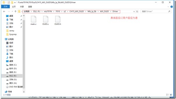
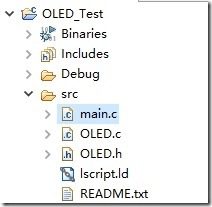
Step4:展开OLED_Test,在Src下按Ctrl+V将所有文件粘贴过来。
Step5:右击工程,选择Debug as ->Debug configuration。
Step6:选中system Debugger,双击创建一个系统调试。
Step7:设置系统调试。
Step8:单击运行程序按钮 运行程序,此时可在OLED上观察到滚动显示我们定义的字符。
15.6 本章小结
本章的方案虽然不及14章的功能强大,但是可以提高CPU的工作效率,充分发挥PL的硬件资源的能力,减轻CPU的负担。
两种方案各有优缺点,前者很好地平衡了PS和PL部分的工作,但是功能单一,只能够显示字符;后者未能合理使用PL资源,但是灵活度高、功能强大。读者可以尝试将两种方案进行融合,取长补短,设计出更优秀的方案。
最新文章
- ABP框架 - 动态Web Api层
- 前端React开发入门笔记
- iOS获取当前app的名称和版本号
- P1119: [POI2009]SLO
- Apache Shiro Architecture--官方文档
- Object-C — KVO & oc通知
- org.springframework.web.context.ContextLoaderListener 转
- Android Cursor类的概念和用法
- MBProgressHUD详解
- DB INIT IN WINDOWS (FOR 12C)
- 逻辑卷管理lvm
- linux 内存 大于 jvm xmx
- 【微软大法好】VS Tools for AI全攻略(3)
- css direction 属性简介与实际应用。
- Oracle 创建,查询,删除 job
- A - 最大子矩阵 HYSBZ - 1084 (DP)
- Linux命令:lsof
- 我有特殊的Windows激活姿势
- show master status, show slave status中的Executed_Gtid_Set
- fcitx、ibus、scim