SLVA299A : Load Disconnect ( Input to Output Isolation ) for the TPS61040
http://www.ti.com/lit/an/slva299a/slva299a.pdf
Many boost converters have an external rectifier diode.
The input voltage of the TPS61170 main boost converter is connected to the output voltage when the device is disabled.
Due to the direct pass from the input to the output, the input supply is not isolated from the output voltage when the IC is disabled.
This application report describes how to use a PMOS transistor to disconnect the boost converter’s input voltage from the output voltage
(known as load disconnect or input to output isolation) when the device is disabled.
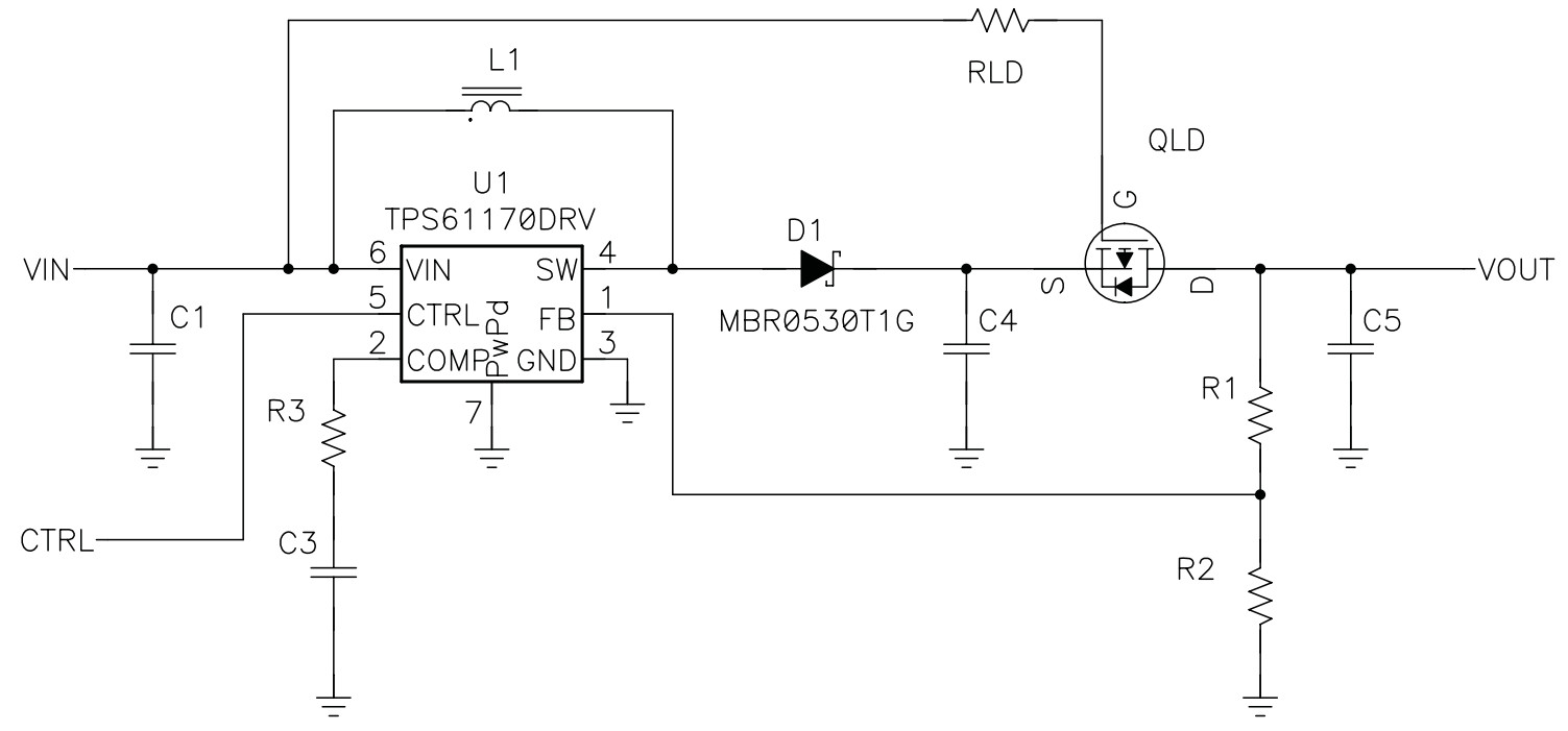
Figure 1 shows the schematic for a TPS61170EVM (SLVU222) that has been modified to include a PMOS transistor Q(LD), and a resistor R(LD)
which form the load disconnect circuit. Capacitor C4 is the minimum capacitor necessary for control loop stability, and C5 represents additional load capacitance.
The boost converter's diode is connected to the source of Q(LD), but the feedback network and output capacitor are connected after Q(LD).
This allows a regulated output voltage even with the use of the transistor Q(LD).
Select Q(LD) to have the following characteristics:
1. a VSD breakdown voltage higher than VOUT
2. a VGS breakdown voltage higher than VOUT – VINmin
3. a low drain to source resistance (RDS(on)) such that the voltage drop created by the maximum output current (IOmax) times RDS(on)
does not take the output voltage below the required minimum regulated voltage for the application.
Capacitor C4 provides a defined bias operation point for Q(LD) and can should be in the 0.1uF to 1uF range.
R(LD)of approximately 100 Ω is recommended to prevent the input voltage from capacitively coupling to the boost converter output.
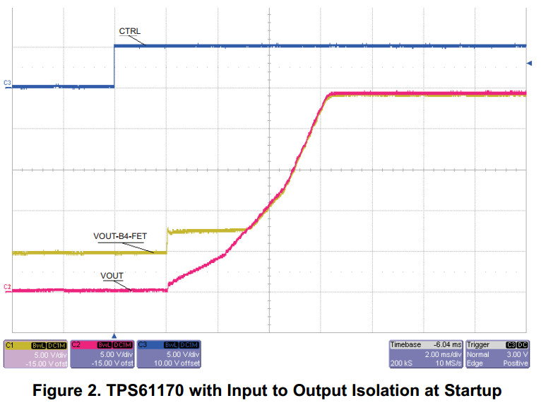
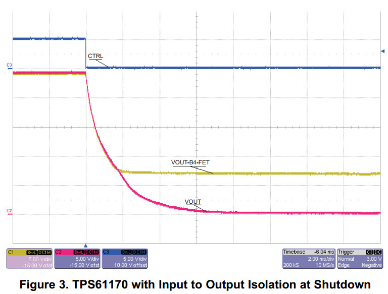
UsingFigure 1 with VIN = 5V and VOUT set to 24 V by R1 and R2, and RLOAD = 240 Ω (IOUT = 100 mA),
Figure 2 shows the circuit starting up while Figure 3 shows the circuit at shutdown.
In both figures, CH1 shown in yellow and set to 5 V/div, shows output voltage before Q(LD) ,
CH2 shown in pink and set to 5 V/div, shows the output voltage after Q(LD), and
CH3 shown in blue, shows CTRL.
Note that the load regulation at large loads is degraded by the IOUT × RDS(on) drop across the FET, i.e.,
VOUT = VREF × (1 + R1/R2) – IOUT × RDS(on).
Note also that efficiency will be degraded slightly due to the IOUT 2 × RDS(on) additional power loss across the FET,
i.e. η = ((VREF × (1 + R1/R2) – IOUT × RDS(on)) × IOUT)/(VIN × IIN).
In this example, the Si2343 -30-V PFET with RDS(on)= 45 mΩ at VGS = 10V was used.
So, with VIN = 12V, the change in load regulation and efficiency is negligible.
At lower input voltages, higher currents, or when using FETs with higher RDS(on), the degradation in load regulation and efficiency is more apparent.
最新文章
- mysql-Federated存储方式,远程表,相当于sql server的linked server
- 《与小卡特一起学Python》 Code2
- MySQL5.6:基于GTID的主从复制
- build.xml配置编译打包过程(转)
- .net微信公众号开发——基础接口
- Android(java)学习笔记66:实现Runnable接口创建线程 和 使用Callable和Future创建线程
- C#实现多国语言的界面切换
- 使用Code::Blocks配置Python编译环境
- UI组件
- Phplot--一些记录
- 用java写的一个简易记事本
- [论文阅读] Deep Residual Learning for Image Recognition(ResNet)
- github错误:fatal: remote origin already exists.
- Monkey测试记录
- CCF CSP 201609-2 火车购票
- mysql 中出现:不能打开到主机的连接,在端口3306: 连接失败
- [PC]两个蓝牙耳机同时输出相同音源
- 【POJ3090】Visible Lattice Points
- EasyUI动态修改easyui-textbox验证信息
- 注解之@PathVariable