RF layout check list
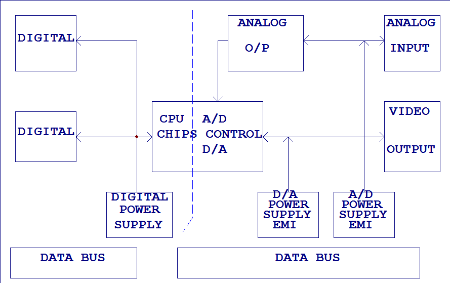
Analog-digital circuit
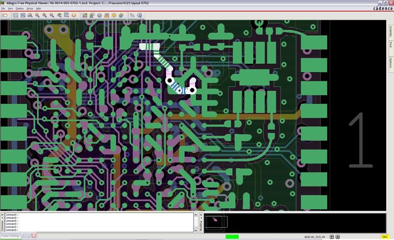
1. Insure C36 and C33 placed next to each other to avoid open stubs
2. Keep UART lines away from 26 MHz traces
3. Keep 26 MHZ traces away from all noisy signals including UART and PCM as well as FM VDD and FM RF PORT
4. Keep 32 KHz trace away from all noisy signals
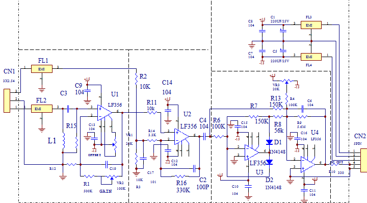
5. The routing and placement of C39 & C45 are very critical to the PA performance:
PAA needs 0.1uF, and PAG needs 1uF.
In terms of layout, PAA and PAG branches stay separate on all layers. Keep branches separate as long as possible all the way back to the main 3.3V Boost supply.
Keep the PAG trace as wide as possible, with a minimum of 2 via for any layer changes.
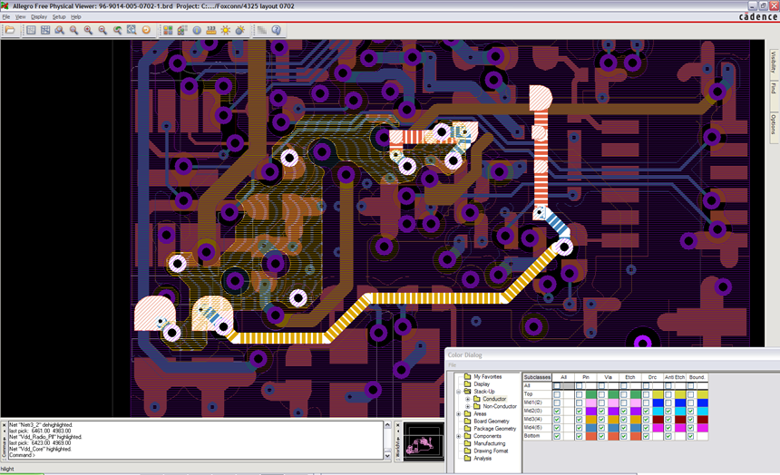
6. place 8.2pF capacitor close to BT_VDDTF pin C42 to L14
7. place a .1uF bypass capacitor on BT_VDDO pins C29 to G8&N2
8. Place a 1000pF capacitor near BT_VDDPLL pin C69 to P14
9. Isolate BT_VDDC from the VDDC rail with a 600 OHM FB do not pace any bypass caps on these pins
10. It is VDD_2P5 in this schematic Also place this capacitor close to the chip and keep away from all noisy components keep the trace to FM VDD as short as possible
11. As on the previous review, please keep the VPP of 32KHz clock < 1.8V from FM RF perspective. VDDIO is rated from 1.8V to 3.3V as addressed on the datasheet. Check with this LPO vender for the spec.
12. Place .01uF bypass cap near FM_VDD VCO C11 to M10
13. Thanks for the change. Again, the routing and placement of C39 & C45 are very critical to the PA performance: C39 to PAG C45 to PAA
PAA needs 0.1uF, and PAG needs 1uF.
In terms of layout, PAA and PAG branches stay separate on all layers. Keep branches separate as long as possible all the way back to the main 3.3V main supply.
Keep the PAG trace as wide as possible, with a minimum of 2 via for any layer changes.
14. L10 should be placed close to the chip output A3 &A1. C22 could be placed close to A3 &A1 or L10.
15.Move C35 close to chip input pins in the layout.
16. VDDIO_RF needs to isolate from VDDIO_SD and VDDIO. Need to use VDD3_3 for VDDIO_RF, and use regulated vdd3_3_ext to power VDDIO_SD and VDDIO.
17. Move C35 close to chip input pins in the layout.
18.Remove C19 & C53. They won't be needed for most of the cases.
最新文章
- CSS3_01之选择器、Hack
- python之RabbitMQ
- Windows 服务开发框架介绍 - Topshelf
- C++ 线程类的一个实现
- 你不知道的JavaScript 二
- JMeter在里面Json数据处理方法
- Arc engine - Geodatabase.
- 驱动力—— 通信引擎(上)—— ESFramework 4.0 进阶(03)
- Salt: Master server cannot see any Minion
- huffman树即Huffma编码的实现
- 30)django-ORM(元信息,级联删除,正反向操作,连表查询优化)
- Centos6.5部署Sonar6.7.1备注
- Python基础学习(五)
- TensorFlow Google大会总结
- Elon Musk
- Mac 下,修改plist文件
- SVN错误:Attempted to lock an already-locked dir及不能提交.so文件
- Glassfish Password Alias
- Ubuntu 安装 phpredis扩展
- 如何理解JavaScript中的this关键字